显示标签为“molybdenum sputtering target”的博文。显示所有博文

2021年4月8日星期四

Molybdenum Sputtering Target Is Essential for Semiconductor Chip

Nowadays, sputtering targets have a wide range of applications, from semiconductor chip to the film deposition of various materials in integrated circuit processing, to energy-saving glass, familiar golden tungsten carbide coting made of titanium nitride and wire-resistance coatings for tools and daily necessities. Many materials can be obtained in the form of sputtering targets during fabrication of CDs and DVDs. 

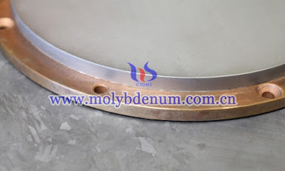
molybdenum sputtering target image

Sputtering is a mature technology, which can deposit films of various materials on many shapes and sizes of substrates. This process is repeatable and can be extended from small projects to the production of medium and large substrate areas. The sputtering gas is usually an inert gas, such as argon. In order to effectively transfer momentum, the mass of the incident particles must match the mass of the target.

In order to obtain the required characteristics in the sputter-deposited film, the materials and processes used to manufacture the sputtering target are critical. In addition to pure metal targets such as tungsten, molybdenum, niobium, titanium, and silicon, there are also alloy targets and compounds such as oxides or nitrides. The process of determining the material is as important as the deposition operating parameters perfected by engineers and scientists during the coating process.

molybdenum sputtering target image

The sputtering target is usually with round or rectangular shapes, other shapes including square and triangular designs also can be customized. The substrate is the object to be coated, which can include semiconductor wafers, solar cells, optical components or many other possibilities. The thickness of the coating is usually in the range of angstroms to micrometers, and the film can be a single material or multiple materials in a multilayer structure.

As a refractory metal with a very wide range of uses, molybdenum has excellent mechanical properties, low expansion, high thermal conductivity and extremely high electrical conductivity at high temperatures. As a sputtering target, it can be many possibilities, such as pure molybdenum target, molybdenum titanium target, molybdenum tantalum target, molybdenum alloy target (such as TZM plate). The molybdenum sputtering target has the characteristics of high purity, high density, uniform fine crystal grains, so as to obtain extremely high sputtering efficiency, uniform film thickness and smooth etching surface during sputtering.

molybdenum sputtering target image

All target products in Chinatungsten Online are specially designed to operate reliably during the film deposition process. Our manufacturing process can ensure high purity, fine and uniform grain size of the target material. We offer a variety of choices of purities and shapes according to your requirements. 

If you have any inquiry of TZM plate, please feel free to contact us:
Email: sales@chinatungsten.com/sales@xiamentungsten.com
Tel.: +86 592 5129696/+86 592 5129595
Fax: +86 592 5129797

Scan QR code of Chinatungsten Wechat platform to follow up the daily latest price and market of tungsten, molybdenum and rare earth.

2021年4月1日星期四

Molybdenum Sputtering Target for Flat Panel Displays, Marking China’s Breakthrough on This Technology

China has developed the first G6 super-large high-end molybdenum target with completely independent intellectual property rights, and put into mass production in 2018. This means that China is the first country that can produce super-size target for semiconductors in the Asia-Pacific region, and breaks the European monopoly on this core technology.

molybdenum sputtering target image

As we all known, limited by equipment and technology, China have to import a large number of this kind of product every year, but now, the breakthrough means that China has taken a crucial step in the localization of core materials for high-end displays.

You may not know the connection of target and our daily life. Actually, they are everywhere in our daily such as smartphones, tablets and color TVs. Molybdenum target, also known as molybdenum sputtering target, it is one of the core materials of the semiconductor industry, more specifically, it is the key core raw material in LCD flat panel displays. In the modern life, we spend several hours or even more than ten hours in a day with it. That’s right, ‘it’ is the mobile phone OLED screen. 

It is proved that materials are the foundation for all products. High-end products and high-tech products have higher requirements for them. You may be a little curious why molybdenum is one of the preferred materials for sputtering targets.

flat panel displays image

Chromium was previously used as the wiring material for flat-panel displays, but it can no longer meet the higher requirements with the advance of technology. For molybdenum material, it has good advantages of high melting point, high conductivity and good corrosion resistance, and its specific impedance and film stress are only 1/2 of that of chromium. In addition, molybdenum is an environmentally friendly material. Therefore, molybdenum has become one of the preferred materials for sputtering targets for flat panel displays. Experts expressed that molybdenum material can greatly improve the brightness, contrast, color and other performance of liquid crystal displays and extend their service life.

As a professional manufacturer of tungsten and molybdenum over two decades, Chinatungsten Online can not only offer molybdenum target, molybdenum alloy targets, but also can offer tungsten and related targets. 

If you have any inquiry of molybdenum sputtering target, please feel free to contact us:
Tel.: +86 592 5129696/+86 592 5129595
Fax: +86 592 5129797

Scan QR code of Chinatungsten Wechat platform to follow up the daily latest price and market of tungsten, molybdenum and rare earth.