2023年5月31日星期三

Molybdenum Electrode Price in June 2023

Ø60x650mm molybdenum electrode price is 1,500.00 USD/PC in early June 2023. This kind of electrode has been widely used in glass melting for many years. 

The electrode made of molybdenum has good advantages of high melting point, high strength and hardness at high temperature, as well as good electrical and thermal conductivity and good corrosion resistance. The use of moly electrodes to replace the original heavy oil and gas energy can effectively reduce environmental pollution and improve the quality of glass. Molybdenum electrode rod is a kind of molybdenum electrode product, its surface is bright gray metallic luster with density more than 10.15g/cm3. They are mainly used for electric glass furnaces, electric light sources and electric vacuum parts.

If you have any inquiry of molybdenum electrode, please feel free to contact us:
Email: sales@chinatungsten.com/sales@xiamentungsten.com
Tel.: +86 592 5129696/+86 592 5129595
Fax: +86 592 5129797

Scan QR code of Chinatungsten WeChat platform to follow up the daily latest price and market of tungsten, molybdenum and rare earth.

Cu/Mo/Cu Carrier Price in June 2023

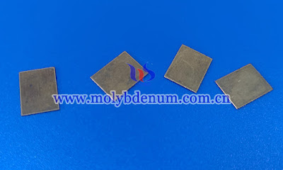
8.6x11x0.5mm Cu/Mo/Cu carrier price is 4.00 USD/PC in early June 2023. These carriers are mainly used in radio frequency, microwave and semiconductor high-power devices, carriers, lead frames, low-expansion layers and heat conduction channels of multilayer printed circuit boards (PCBs).

Cu/Mo/Cu carrier price photo

Cu/Mo/Cu carrier (CMC) is a composite material with a similar sandwich structure, the core material is molybdenum, and both sides are covered with copper. The basic concept of the design is to use the high thermal conductivity of copper and the low thermal expansion characteristics of molybdenum. By adjusting the thickness ratio of copper, molybdenum and copper, it can achieve a thermal expansion coefficient matching ceramic materials and semiconductor materials, and a higher thermal conductivity. The expansion coefficient and thermal conductivity are designable.

The ideal carrier material should have a linear expansion coefficient CTE, which is basically matched with the chip, and has the highest possible thermal conductivity, especially the Z-direction (thickness) thermal conductivity, so that the heat of the packaged chip and other electronic devices can be quickly discharged. In order to increase its power density, achieve high power, reduce the volume and realize the miniaturization of the device. CMC material is now the one of the materials to meet above requirements.  

If you have any inquiry of molybdenum copper carrier, please feel free to contact us:
Tel.: +86 592 5129696/+86 592 5129595
Fax: +86 592 5129797

Scan QR code of Chinatungsten WeChat platform to follow up the daily latest price and market of tungsten, molybdenum and rare earth.

2023年5月4日星期四

Molybdenum Sheet Price in May 2023

The latest price of 0.1x300x1500mm molybdenum sheet is USD100.00/PC, EXW XIAMEN, CHINA in May 2023. 

molybdenum sheet price photo

When your applications require an element with a high melting point, high temperature strength, low coefficient of expansion and low vapor pressure at elevated temperatures, molybdenum is the material of choice. Molybdenum sheets can be used to manufacture electric light source parts, electric vacuum components and power semiconductors, as well as molybdenum boats, heat shields, and heating elements of high temperature furnaces.

Chinatungsten Online is the world's leading supplier of high-quality molybdenum sheet products, and can provide cold-rolled sheet products of various thicknesses and lengths according to customer requirements. Like all of our materials, our sheets start with metal powder, which is then pressed into ingots, sintered, and then rolled. This process allows us to customize products to meet specific material and performance requirements to ensure optimum performance in your application.

If you have any inquiry of tungsten sheets, please feel free to contact us:
Email: sales@chinatungsten.com/sales@xiamentungsten.com
Tel.: +86 592 5129696/+86 592 5129595
Fax: +86 592 5129797

Scan QR code of Chinatungsten WeChat platform to follow up the daily latest price and market of tungsten, molybdenum and rare earth.

Molybdenum Crucible Price in May 2023

The latest price of φ250x300mm molybdenum crucible is USD12,000.00/PC, EXW XIAMEN, CHINA in May 2023. 

molybdenum crucible price photo

Corrosion resistance, creep resistance and high temperature performance make molybdenum made crucibles very suitable for high temperature crystal growth processes. When sapphire is easy to extract, higher sapphire yield and quality can be achieved. The molybdenum-based crucible has heat resistance and a smooth surface, making it durable and cost-effective.

The surface roughness of the molybdenum crucible needs to be higher than 1.6 µm. When the surface of the crucible is rough, the sapphire is not easy to take out and it is easy to damage the crystal. In addition, the crucible will be damaged in the process. Chinatungsten Online's ultra-smooth crucible eliminates these problems. Sapphire manufacturers can benefit from this product because it eliminates complex and expensive processes. In addition, the smooth surface is resistant to corrosion caused by aggressively molten sapphire. This function can extend the service life of reusable crucibles.

Moly crucibles for sapphire growth furnaces are available with a variety of dimensions including round, in numerous standard diameters and wall thicknesses. Custom configurations are available. In addition, many other components for these furnaces are also customized.

If you have any inquiry of molybdenum crucible, please feel free to contact us:
Email: sales@chinatungsten.com/sales@xiamentungsten.com
Tel.: +86 592 5129696/+86 592 5129595
Fax: +86 592 5129797

Scan QR code of Chinatungsten WeChat platform to follow up the daily latest price and market of tungsten, molybdenum and rare earth.

2023年5月3日星期三

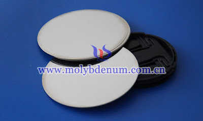
Molybdenum Wafer Is Used as Heat-sinker for LED chips

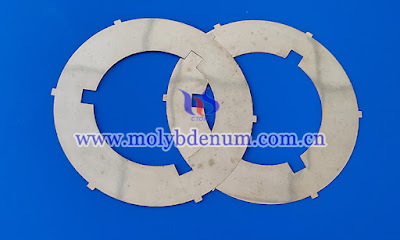
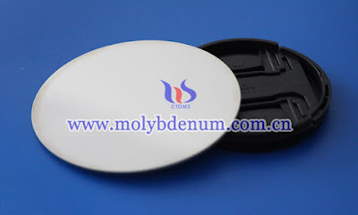
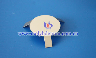
Molybdenum wafer is a circular sheet made of molybdenum material, usually with a diameter of 0.1mm to 2.0mm. It usually has high density, good mechanical properties and corrosion resistance, and can be used to manufacture various high-temperature and corrosion-resistant parts. 

From the point of view of appearance, they are generally dark brown, but after alkali washing, they are usually silver gray with high gloss. The surface is smooth and flat, without heavy skin, delamination, inclusion of impurities, and cracks, and defects such as cracked edges.

molybdenum wafer image

From the point of view of physical and chemical properties, they have high melting point (2620°C), density (10.2g/cm3), hardness (Mohs hardness is 5~5.5) and strength, lower coefficient of thermal expansion and resistivity, and higher high conductivity, good chemical stability, high temperature creep resistance, oxidation resistance, high temperature resistance and corrosion resistance.

There are two main production methods for molybdenum wafers, one is powder metallurgy, and the other is cold rolling. The powder metallurgy method is to mix molybdenum powder with other alloying elements, and then form it into wafers by pressing. The cold-rolling method is to make molybdenum plate blanks through high-temperature and high-pressure rolling, and then perform annealing and alkali cleaning to obtain thin molybdenum sheets. 

molybdenum wafer image

As molybdenum has the characteristics of high melting point, high strength, high hardness, low thermal expansion coefficient and excellent corrosion resistance, molybdenum wafers are widely used in aerospace, electronics, semiconductor, chemical and other fields, such as for the manufacture of vacuum furnace interior components, high-temperature heating elements, X-ray tube windows, linings of molten glass kettles, etc. In addition, our pure molybdenum is the ideal materials as heat-sinker for bonding to LED chips.

Chinatungsten Online is a professional manufacturer of tungsten and molybdenum for more than two decades. We can supply various dimensions of molybdenum discs or molybdenum waters as per the drawings. Please free feel to contact us when you get any purchasing plans.

If you have any inquiry of molybdenum wafer, please feel free to contact us:
Email: sales@chinatungsten.com/sales@xiamentungsten.com
Tel.: +86 592 5129696/+86 592 5129595
Fax: +86 592 5129797

Scan QR code of Chinatungsten WeChat platform to follow up the daily latest price and market of tungsten, molybdenum and rare earth.

Why Molybdenum Wafer Can Be for Bonding to LED Chips?

Molybdenum wafer is a flake-shaped molybdenum material, usually with a thinner thickness and larger diameter. It is usually used in applications under high temperature, high pressure and strong corrosive environment, such as aviation, aerospace, electronics, chemical industry and other fields, and is manufactured through molybdenum material processing technology, such as rolling, drawing and other methods.

It can vary in size depending on specific application needs. Normally, its thickness can range from 0.05mm to 10mm, and the diameter can be large to 300mm. For some applications with special requirements, the size of the molybdenum wafer may need to be larger or smaller, and more precise control is also required. Its size can be selected according to the standard size provided by the manufacturer, or can be customized to meet the specific application requirements.

molybdenum wafers photo

There are many characteristics of this material as following: 

High melting point: the melting point of molybdenum is 2610°C, which is one of the highest melting points among all metals.

High hardness: its Mohs hardness is between 6.5 and 7.5, which is harder than ordinary steel.

Good corrosion resistance: it can be used in some strongly corrosive environments, such as strong acid and strong alkali environments.

Low thermal expansion coefficient: its thermal expansion coefficient is relatively small, relatively stable, and can be used at high temperatures.

Good electrical conductivity: it can maintain good electrical conductivity at high temperature.

molybdenum wafers photo

High strength: it has high strength and can withstand large external forces. At the same time, it has good toughness and are not easy to break.

A light-emitting diode (LED) is a semiconductor device that emits visible light when an electric current passes through it. Pure molybdenum is the ideal material as carrier wafers for bonding to LED chips because of the above good characteristics. 

Chinatungsten Online is a professional manufacturer of tungsten and molybdenum for more than two decades. We can supply various dimensions of molybdenum discs or molybdenum waters as per the drawings. Please free feel to contact us when you get any purchasing plans.

If you have any inquiry of molybdenum wafers, please feel free to contact us:
Email: sales@chinatungsten.com/sales@xiamentungsten.com
Tel.: +86 592 5129696/+86 592 5129595
Fax: +86 592 5129797

Scan QR code of Chinatungsten WeChat platform to follow up the daily latest price and market of tungsten, molybdenum and rare earth.
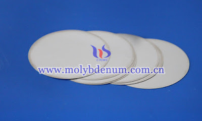
Molybdenum Wafers Are Used as Substrates of Silicon Controlled Rectifier (SCR)

Molybdenum wafers are made of pure molybdenum material with purity over 99.95%, which can be used in high temperature technology, electronic devices, aerospace, chemical industry, and other fields due to their characteristics of high temperature, high strength and high stability.

The processing technology can be referred to the following: 

Cutting: the original material of wafers can be in forms of plates, strips or rods, which need to be cut according to the required diameter and thickness of the wafers. Cutting can be done by mechanical shearing or laser cutting.

molybdenum wafers image

Extrusion or cold rolling: wafers need to be deformed to obtain the required dimensions and properties. Extrusion or cold rolling are commonly used texturing methods that allow the wafer to achieve a smaller thickness while increasing its strength and hardness.

Finishing: the surface of the wafer needs to be finished, usually by grinding and polishing, to eliminate the surface defects that may be left in the process of cutting, extrusion or cold rolling, and improve the surface finish and flatness of the wafer.

Cleaning and packaging: they need to be cleaned after processing to remove impurities and residues generated during processing. After cleaning, they need to be packaged, usually with anti-rust paper and plastic bags to protect the surface from oxidation and pollution.

molybdenum wafers image

Molybdenum wafers are mainly used as substrates of silicon controlled rectifier (SCR). Because there are many types of silicon rectifiers with different specifications, the specifications as substrates are also relatively wide. The diameter is generally 4-100mm and the thickness is 0.1-3.0mm. However, with the continuous and rapid development of the semiconductor industry, the market demand for moly wafers larger than φ76.2mm, such as φ100mm, is increasing year by year.

Chinatungsten Online is a professional manufacturer of tungsten and molybdenum for more than two decades. We can supply various dimensions of molybdenum discs or molybdenum wafers as per the drawings. Please free feel to contact us when you get any purchasing plans.

If you have any inquiry of molybdenum wafers, please feel free to contact us:
Email: sales@chinatungsten.com/sales@xiamentungsten.com
Tel.: +86 592 5129696/+86 592 5129595
Fax: +86 592 5129797

Scan QR code of Chinatungsten WeChat platform to follow up the daily latest price and market of tungsten, molybdenum and rare earth.

What Are Differences Between Molybdenum Wafer and Molybdenum Sheet?

Molybdenum wafer and molybdenum sheet are both molybdenum products with thin thickness and similar production processes and applications. However, they also have differences as following: 

Shape and size: moly wafers are circular flakes made of molybdenum materials, usually with a diameter below 3.0mm and the moly sheet is a rectangular sheet, which is usually thicker than water. The maximum width is about 600mm but the length can reach 3000mm. 

molybdenum sheet image

Applications: they have different uses due to their different shapes and sizes. Moly wafers are usually used to make some small, high-precision parts, such as vacuum furnace internal components, high-temperature heating elements, X-ray tube windows, etc.; while moly sheets are usually used to manufacture some larger structural parts that need to bear a certain load, such as propellers and turbine blades in the aerospace field.

Manufacturing process: the processing technology of moly wafers is relatively complicated, and precise machining equipment and technology are required to ensure its dimensional accuracy and surface quality. The processing technology of molybdenum sheet is relatively simple, and can be processed by stamping, bending, shearing and other processes.

molybdenum wafer image

The annual consumption of moly wafers in China is 80-100 tons, and the annual consumption of molybdenum sheets is 107-133 tons. Because the consumption of wafers is closely related to the development of the power semiconductor industry, the demand for follow-up this metal wafer is expected to increase. 

Chinatungsten Online is a professional manufacturer of tungsten and molybdenum for more than two decades. We can supply various dimensions of molybdenum discs, molybdenum sheets, molybdenum plates and molybdenum wafers as per the drawings. Please free feel to contact us when you get any purchasing plans.

If you have any inquiry of molybdenum wafer, please feel free to contact us:
Email: sales@chinatungsten.com/sales@xiamentungsten.com
Tel.: +86 592 5129696/+86 592 5129595
Fax: +86 592 5129797

Scan QR code of Chinatungsten WeChat platform to follow up the daily latest price and market of tungsten, molybdenum and rare earth.